PCB Manufacturing and PCB Design has been changing a lot in the last years, the first circuit board designs were quite simple, but new technologies, have brought new performance needs to the Printed Circuit world, and the design and fabrication practices have become more sophisticated. One of these practices is Controlled Impedance in PCB Fabrication, which is intended to vary from the amount of power to the speed of a signal in the Circuit traces.
WHAT DOES IMPEDANCE MEAN
The degree of opposition to the flow of energy in an electrical circuit, or transmission line, is expressed in Ohms and known as impedance. It is the result of summing the resistance and the reactance of an electrical circuit, with the reactance being consequence of two effects.
- Inductance: Induction of voltages in conductors, due to the magnetic fields of currents.
- Capacitance: Electrostatic charges' storing, due to the voltages among conductors.
At low frequencies (DC), the reactance become negligible and the impedance is merely formed by the resistance, but for high frequency circuits the reactance and therefore the impedance become a very important factor.
WHAT IS CONTROLLED IMPEDANCE
Impedance mismatches in a system, lead to glitches and reductions in the system's performance levels. Assuring that impedance mismatches are within tolerable limits, is a design feature usually known as Controlled Impedance.
A common example of this feature is the design of a coaxial cable: formed by an inner conductor separated, using an insulator, from the shield (an outer cylindrical conductor). The electrical characteristics of the insulator, along with all components' proportions are carefully controlled to regulate the impedance level of the cable.
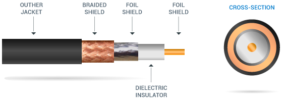
Correspondingly, in PCB Manufacturing, the traces represent the conductor, the laminate represents the insulator and the planes represent the shield. Therefore, the impedance of a printed circuit board depends on the dimensions and materials used in the fabrication process.
WHY IS CONTROLLED IMPEDANCE SO IMPORTANT?
The purpose of a trace, in a Printed Circuit Board, is to transfer the maximum signal power from source to load, but this assignment can only be achieved when the impedance value of the source matches the impedance value of the load, otherwise a portion of the signal's energy will be reflected to the source, degrading its quality. With today's fast rise time signals, the design of Circuit Boards with controlled impedance has become very popular.
HOW IT IS DONE?
The impedance control in Printed Circuit Board Fabrication and Design is accomplished by two means: a well-defined PCB Stack-up and careful trace design. It is known that Impedance is proportional to laminate height and inversely proportional to trace width and thickness. Consequently, varying the sizes and spacing of a specific trace will adjust its impedance value.
Impedance depends also on the dielectric constant of the laminate: A number used to quantify the inherent ability of a material to store electrical energy in an electric field. The most common configurations for controlled impedance traces are Stripline and Microstrip, and their different geometries can be seen in the following figure.
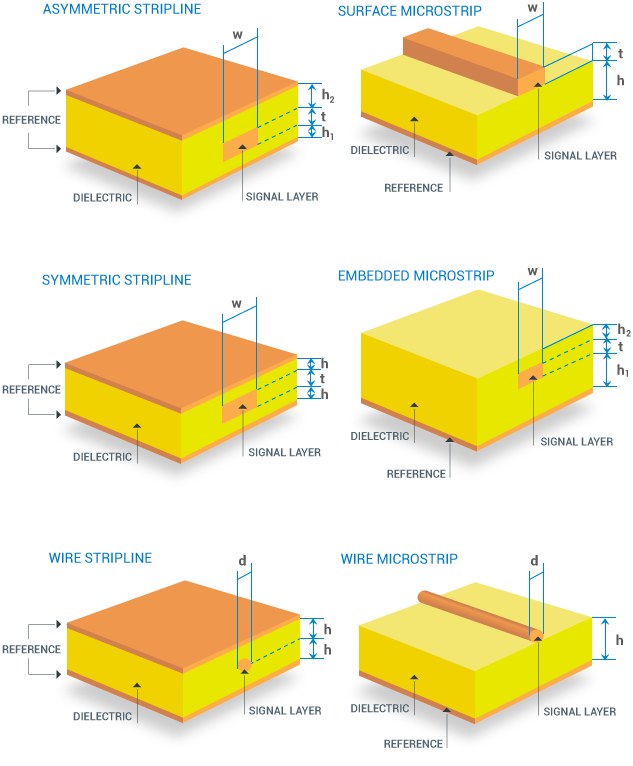
Microstrip involves a signal trace separated from a reference plane (ground plane) by a dielectric layer. There are different microstrip configurations, in the simplest case the signal trace is placed on the surface of an outer dielectric layer surrounded by a solder mask or the air. For thin traces, the soldermask will affect the impedance of a microstrip, reducing its value by 2 to 3 ohms. Stripline consists of a signal trace surrounded by a solid dielectric that separates the trace from two reference planes.
I.C.T is a manufacturer of SMT machines. It mainly provides customers with SMT production lines including SMT Stencil Printers, Pick and place machines, Reflow Oven, AOI Machine, Wave Soldering Machine and PCB Handling Machine etc. I.C.T has more than 25 researches on SMT and DIP technology, for the world Customers provide SMT total solutions. There are successful cases of SMT technical team in Asia, Europe, America, Africa, and Australia.
I.C.T provide SMT solutions at various stages according to the different needs of customers. I.C.T is not only a provider of SMT equipment and technology, but also is the customer's escort in the field of SMT and DIP.
Welcome more people to discuss with us about SMT technologies and solutions, please contact us for more information:
Tel: +86 13670124230 (WhatsApp/Skype/WeChat)
Email: etasmt@foxmail.com
Keywords:
Mobile SMT Line, SMT Assembly Line Mini, Stencil Printer Inspection, SMT Semi AutomatIC Paste Printing Machine, Vapour Phase Oven, Vapor Phase Oven, Flux Sprayer DIP Soldering Machine, Low Cost SMT PICk And Place PCB Assembly, Hanwha/Hanw Ha PICk And Place Machine Sm482Plus, Juki Jx-100 PICk And Place Machine, 8MM ElectrIC Feeders For SMD PICk And Place, PICk-And-Place Machine , Coating Machine Dispensing For SMT For PCB, Coating Machine Dispensing For SMT For PCB LED, Double Digital Coating Machine PCB, 12 Volts Charder Auto Cut Off PCB With Components